NFC is an emerging technology that has developed rapidly in recent years. The technical goal is short-range communication between electronic devices, working in the 13.56MHz frequency band. The emergence of NFC technology has greatly promoted the integration of RFID technology and mobile communication technology, and has led to many new application modes. The SWP solution is a mobile payment solution based on NFC technology.
The single-line connection protocol is mainly used to connect the SIM card of the mobile phone or the communication between the SD card and the CLF. Now it has been recognized by all SIM card manufacturers, and some mobile phone manufacturers have joined the ranks. There are three implementations of the SWP solution, namely the NFC-SIM solution, the NFC-SD solution, and the full terminal solution. At present, UnionPay is the first to promote the SWP-SD solution. China's three major operators, China Unicom, China Telecom and China Mobile, use the SWP-SIM solution as their target solution.
The NFC function implementation of the SWP solution consists of two parts: the NFC analog front end (NFC Controller and antenna) and the security unit. The security unit can be a SIM, SD, SAM or other chip depending on the application requirements. The security unit of the NFC-SIM solution is a SIM card, and the security unit of the NFC-SD is a Micro SD card.
Compared with the dual interface card solution and the film card solution, the SWP solution has the advantage that the SWP related specifications are international specifications, and the industrial chain is relatively mature, and supports three working modes of the NFC technology - the card simulation mode, the card reader mode, and Point-to-point mode.
1. SWP specification system
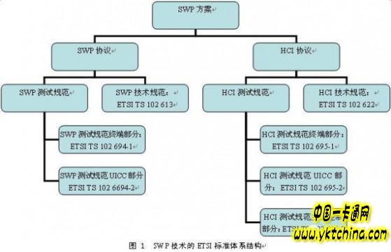
At present, the SWP solution has mature technical requirements and test methods, and its ETSI standard system is shown in the figure.

2. SWP interface
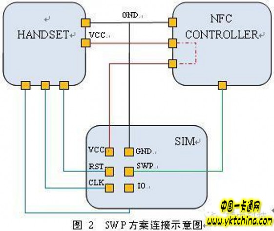
SWP is a C6-pin-based single-wire connection scheme proposed by Gemalto. The figure below is a schematic diagram of the connection of the SWP scheme.

In the SWP scheme, the interface interface includes three lines: VCC (C1), GND (C5), and SWP (C6). One of the SWP signal lines implements full-duplex communication based on the voltage and load modulation principle, so that the SIM card can be realized. Both the 7816 and SWP interfaces are supported under the ISO7816 interface definition, and the pins that extend the third high-speed (USB) interface are reserved. The SIM card supporting SWP must support both the ISO and SWP communication protocols, and the two parts need to be managed independently. The RST signal of the ISO interface cannot affect the SWP part. SWP implements full-duplex communication on a single line, defining signals in both S1 and S2 directions. The S1 signal is transmitted through a digitally modulated (low or high) voltage signal, and the S2 signal is transmitted through a digitally modulated (low or high) current signal. The SWP interface has three states: active state, suspended state, and deactivated state. The SWP interface works normally in the active state.
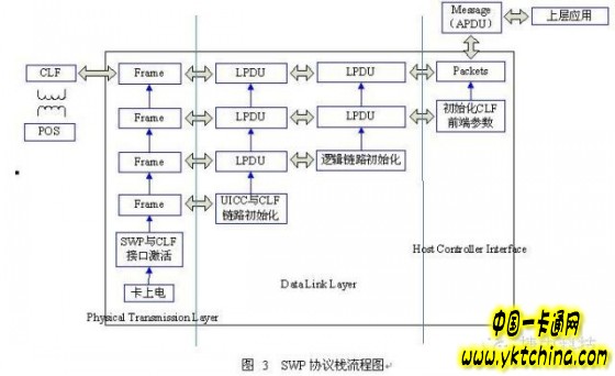
Figure 3 is a general flow diagram of the SWP protocol stack on the smart card. A set of protocols used by a particular system is called a protocol stack. The SWP interface system completes the data transmission with the NFC chip, the bottom layer uses the SWP protocol, and the upper layer uses the HCI protocol. The SWP protocol and the HCI protocol together form the protocol stack of the SWP interface system. The SWP protocol is divided into a MAC layer and an LLC layer, wherein the MAC layer is responsible for frame closing and deframing, and the LLC layer implements frame error management and data interaction control. The HCI layer specifies the technical requirements of the main control interface between the UICC and the contactless communication module (CLF).

Figure 3 SWP protocol stack flow chart
The SWP interface relies on a hardware interrupt driver, and the SWP interface is in a state of waiting for an interrupt before it is activated. When communicating via the SWP interface, the NFC chip is activated upon detection of the presence of the RF field. The NFC chip sends the S1 signal to the SIM card. After the SIM card detects the S1 voltage signal, it triggers the Suspended interrupt notification software to prepare for communication. At this point, the software sets the communication parameters, and then waits for the interruption of the subsequent data to perform the initial activation process of the SWP interface. If the initial activation of the SWP interface is successful, the software starts to negotiate the sliding window size WS of the SHDLC protocol, waiting for the establishment of the SHDLC link. Generally speaking, the window size is determined by the number of hardware receiving and transmitting FIFOs. Assume that the sliding window supported by the card terminal is WS=N, and the NFC chip sends a reset frame supporting the sliding window WS=M. If the M SHDLC link is successfully established. After that, the SWP interface waits for an information frame. After receiving the information frame, the data is read from the RX FIFO according to the number of received bytes of the status register written by the hardware, and then the received data packet is parsed by the software; the data packet is delivered to the application layer through the routing layer of the HCP, and the application layer According to the type of the message, the corresponding processing.
3. Difficulties in the implementation of the SWP protocol stack in smart cards
Whether implementing the SWP-SIM card or the SWP-SD card's incoming payment function, it is necessary to establish a SWP interface for communication with the CLF on the security chip. In addition to the hardware support, the SWP interface is also very important for its software protocol interface. After more than one year of research, on the basis of in-depth study of SWP related technical specifications and test specifications, it is concluded that there are four technical difficulties in the implementation of SWP protocol stack, namely:
(1) In order to ensure that the SWP module has a strong platform portability, the transfer relationship between the layers is simplified as much as possible. The delivery and dependency of the underlying chip and the upper application are implemented with minimal overhead. This also imposes stricter requirements on the definition of programming and functional modules. Moreover, considering the resource usage of the module code, it is necessary to compress the system code space and ram space as much as possible.
(2) In the original security chip operating platform, there is only a single 7816 interface, and there is no dual interface independent mechanism. Under the new design framework, the dual interface is independently operated, and the ATR can be initialized and sent in the 7816 when the SWP is working normally. Or do SWP activation processing at any stage of the 7816 work.
(3) Power consumption problem, the card power consumption is too large on some mobile phones, resulting in the SWP interface not working stably. When the SWP interface is activated, the timing of the card is required. That is, after the VCC is powered on for 1 ms, the S1 signal is raised, and the card must send out the ACT_SYNC frame within 0.7 ms. Moreover, when using the incoming payment function, the response time of the card is required when using the refill and consumption functions in the POS. Therefore, when designing the protocol stack, the CPU operating frequency of the card needs to be considered by many parties, and must meet the requirements of both aspects.
(4) Since the card end and the CLF end are externally represented as non-contact cards, it is necessary to set the non-contact characteristic of the external performance of the CLF end. This will set the CLF to the corresponding contactless transmission mode. This part belongs to the configuration of the HCI layer initialization parameters, and the configuration of the parameters involves compatibility on each mobile phone.
4. Summary and outlook
In recent years, as key technologies such as 3G and 4G have been further promoted in new markets, as well as active expansion plans of various suppliers, the coverage of mobile phone networks has continued to expand, and as the price of smartphones has declined, more and more Consumers choose smartphones with more complete features. Mobile phones are no longer a simple communication tool, and it is expected to integrate communication, entertainment and payment functions in the future.
In China, China UnionPay has achieved very significant results in guiding, supporting and supervising the entire mobile payment industry. The issuance of third-party payment licenses by the central bank regulates the competitive landscape of the industry and is conducive to the healthy development of the entire industry. After China UnionPay, China's three major operators - China Mobile, China Unicom and China Telecom - have finally begun to fully promote the NFC-SWP mode of mobile payment services, and Samsung, HTC and other mobile phone manufacturers have launched support for NFC-enabled A variety of mobile phones. Under the influence of an orderly market environment, many technology equipment providers will also invest more resources in the development of technology. I believe that in the future, "SWP-SIM card products" and "SWP-SD card products" will have better performance and provide more and better products for everyone. At the same time, China's mobile payment will also usher in a broader and brighter development prospects.
Waste Bin,Waste Basket,Garbage Bin,Ss Dustbin
NINGBO ZIXING ELECTRONIC CO.,LTD. , https://www.zixingautobin.com